

Intelligent Systems Division
The NASA Ames Intelligent Systems Division provides leadership in information technologies by conducting mission-driven, user-centric research and development in computational sciences for NASA applications. We develop ground and flight software systems and data architectures for data mining, analysis, integration, and management; integrated health management; systems safety; and mission assurance. We transfer these new capabilities for utilization in support of NASA missions and initiatives.
The Division is part of Ames Research Center’s Exploration Technologies Directorate, which provides advanced technologies for NASA’s Aeronautics Research, Science, Human Exploration and Operations, and Space Technology Mission Directorates, as well as mission support organizations within the Agency. Over 400 NASA civil servant employees, contractors, and student interns work at the division.
Location
Moffett Field, CA
NASA
Ames Research Center
Division Chief
Dave Alfano
Focus Areas and Capabilities
Located at Ames Research Center in the heart of Silicon Valley, the Division comprises four concentrated areas of computer science and information technology research and development: * Autonomous Systems and Robotics * Collaborative and Assistant Systems * Discovery and Systems Health * Robust Software Engineering.
Autonomous Systems and Robotics (ASR)
Enabling complex systems through the development of technologies that can adapt in response to changing conditions, knowledge, and constraints
Collaborative and Assistant Systems (CAS)
Providing collaborative technologies and data systems to manage specialized technical information for NASA Missions, Programs, and projects
Discovery and Systems Health (DaSH)
Understanding, modeling, and reasoning with engineered systems and science data to meet the needs of aerospace missions. Building resilient systems and conducting foundational research in quantum computing, machine learning, and computational materials
Robust Software Engineering (RSE)
Increasing systems safety and performance by enhancing software quality, reliability, and productivity through research done in the context of NASA applications in space, aviation, and wildfire management
Division Information & Resources
Featured Projects
ARMADAS
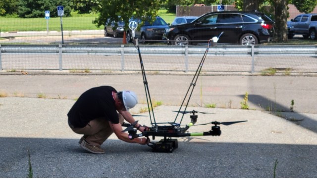
The Automated Reconfigurable Mission Adaptive Digital Assembly Systems (ARMADAS) project has developed an infrastructure that autonomously assembles itself from a set of packed parts. This scalable automated assembly of physical systems is critical to massless exploration and in-space reliance goals, including development of habitat-scale systems, long-duration spaceports, next-generation solar power, communications, and scientific instrumentation. The goal is to change the cost-scaling curve for mission infrastructure relative to size and duration.
More on ARMADAS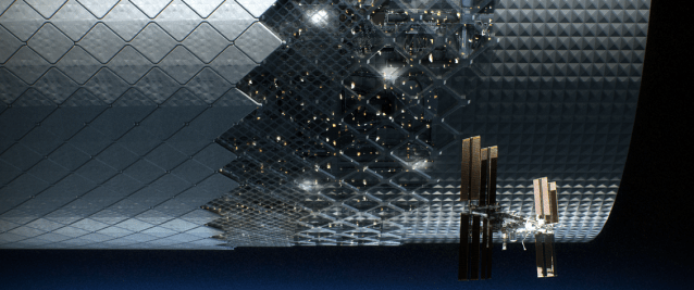
Astrobee
The Astrobees are next-generation free-flying robots that operate in the interior of the International Space Station and can be remotely operated by astronauts in space, or by mission controllers on the ground. Their primary purpose is to provide a flexible platform for research on zero-gravity free-flying robotics, with the ability to carry a wide variety of future research payloads and guest science software. They were also designed to perform a number of Intra-Vehicular Activities (IVAs), including interior environmental surveys (e.g., sound level measurement), inventory, and mobile camera work.
More on Astrobee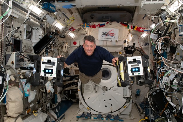
BioSentinel
The BioSentinel mission is one of the secondary payloads to fly on the Space Launch System’s (SLS) first Exploration Mission (EM-1). The primary objective of BioSentinel is to develop a biosensor using a simple model organism (the saccharomyeces cerevisiae strain of yeast is being used) to detect, measure, and correlate with other measurements the impact of space radiation to living organisms over long durations beyond Low Earth Orbit (LEO).
More on BioSentinel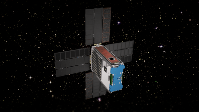
Fluidic Telescope Experiment
The Fluidic Telescope Experiment (FLUTE) is a collaboration involving NASA Ames Research Center, NASA Goddard Space Flight Center, and Technion – Israel Institute of Technology. It aims to revolutionize space astronomy and in-space manufacturing of high-precision optics for a variety of applications by leveraging the physics of wetting and hydrostatic phenomena in microgravity. The approach being developed by the project is scale-invariant and expected to enable space telescopes with optical apertures measuring in tens or even hundreds of meters to directly image extra-solar planets.
More on FLUTE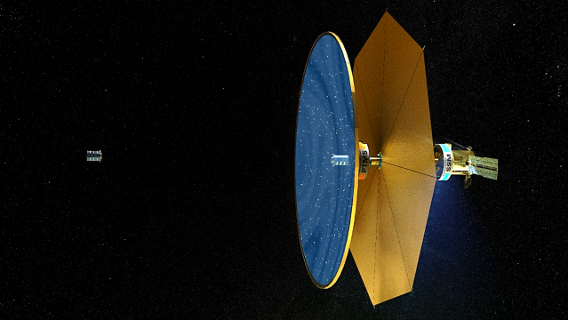
Mission airborne Tools Suite
The Mission airborne Tools Suite (MTS) is a web-based software application that acts as the unified endpoint for many of the key enabling technologies available through the Airborne Science Program (ASP) Sensor Network, including the visualization of mission information sources to aid real-time decision making. MTS is primarily used for observing real-time telemetry from remote sensing airborne platforms in concert with meteorological, airspace, satellite, and other mission products to improve situational awareness for all participants in NASA Airborne Science missions.
More on MTS
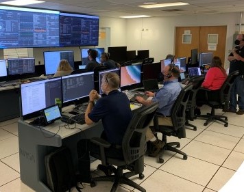
Mission Control Technologies
The Open Mission Control Technologies (Open MCT) platform is a next-generation mission control framework for visualization of mission data on desktop and mobile devices. Developed at NASA's Ames Research Center in collaboration with the Jet Propulsion Laboratory (JPL) and NASA’s Advanced Multi-Mission Operations System (AMMOS). Open MCT is being used by NASA for data analysis of spacecraft missions, including the Mars Cube One (MarCO) missions, the Arcsecond Space Telescope, the Mars 2020 rover testbed, and the Volatiles Investigating Polar Exploration Rover (VIPER).
More on MCT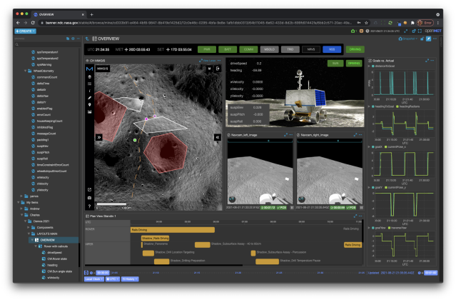
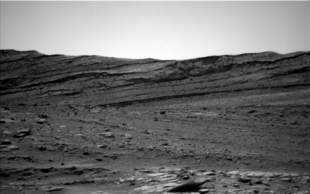
OceanWATERS
The Ocean Worlds Autonomy Testbed for Exploration Research and Simulation (OceanWATERS) software is a simulation environment for research and development of onboard autonomy software for scientific lander missions to the "ocean worlds" of our solar system: the moons harboring large quantities of liquids, such as Europa, Enceladus, and Titan. The proposed "Europa Lander" mission was chosen as a reference design to inform the development of the simulator.
More on OceanWATERS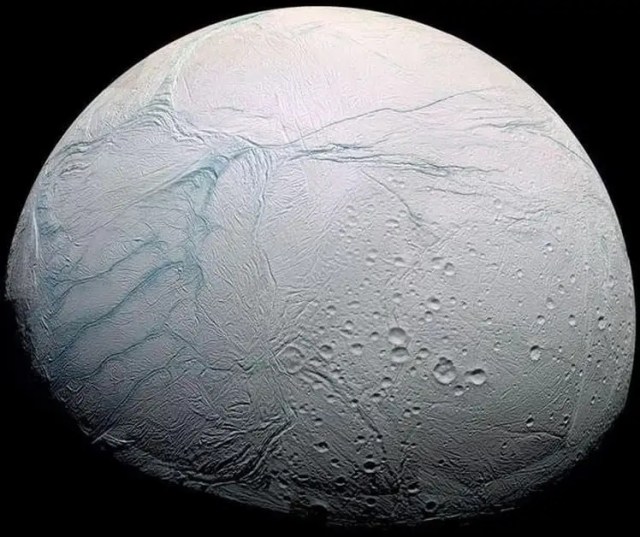
ODIN-fire
The Open Data Integration Framework for Wildland Fire Management (ODIN-fire) is a software architecture to create field-deployable servers that can import, process, and display an open number of wildland fire-related data sources, such as weather, fire location, and near-real-time location of vehicles and personnel. It allows stakeholders to create and run their own fire-related applications, improving situational awareness of wildfires and resources in the field.
More on ODIN-fire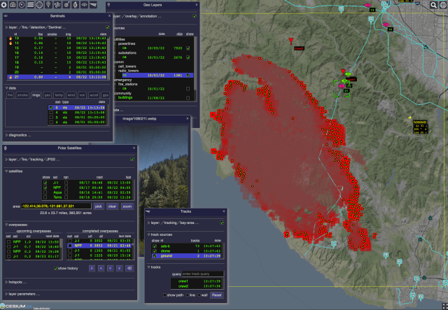
Prognostics Center of Excellence
The Prognostics Center of Excellence (PCoE) at Ames Research Center provides an umbrella for prognostic technology development, specifically addressing prognostic technology gaps within the application areas of aeronautics and space exploration.
More on PCoE
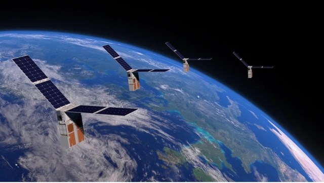
Starling
NASA’s Starling mission is advancing the readiness of various technologies for cooperative “swarms” of spacecraft to enable multipoint science data collection. The six-month mission is using four CubeSats in low-Earth orbit to test four technologies that let spacecraft operate in a synchronized manner without resources from the ground: swarm maneuver planning and execution, communications, relative navigation, and autonomous coordination between spacecraft. The Starling mission extension referred to as Starling 1.5 will demonstrate Space Traffic Management technologies for autonomously controlled constellations over nine months in 2024.
More on Starling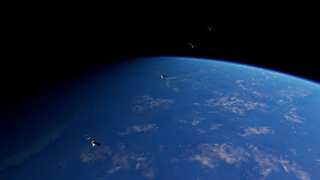
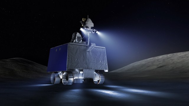
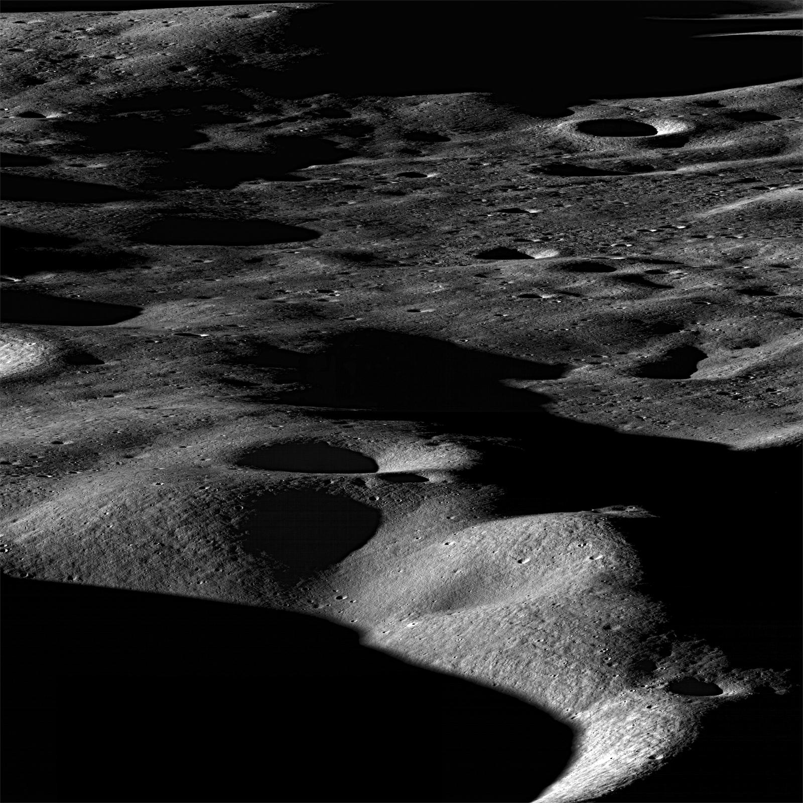
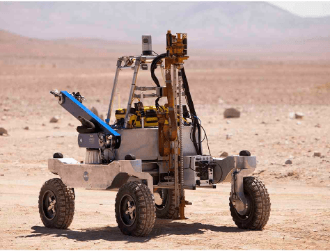
VIPER
After landing near the Nobile Crater on the Moon, the Volatiles Investigating Polar Exploration Rover (VIPER) will travel to investigate a range of Ice Stability Regions (ISRs) across scales from hundreds of meters to kilometers and conduct a surface and subsurface assessment of lunar water and other volatiles. VIPER includes a suite of rover-mounted instruments (three spectrometers and a drill), which the VIPER Science Mission team will use to characterize the nature of the volatiles and to create global lunar water resource maps.
More on VIPER